|
7108
S. Alton Way, Unit I |
(303) 758-2728
Home > Glossary of Terms > S Definitions
Glossary - S's
Scanning electron microscope (SEM) (sc) microscope used to magnify images as much as 50,000 times by means of scanning with an electron beam. The impinging electrons cause electrons on the surface to be ejected. The ejected electrons are collected and translated into a picture of the surface.
Scarf joint (r) a connection made with two ends cut at an angle and overlapping.
Scorch (r) premature vulcanization of a rubber compound.
Scorch, Mooney (r) the time to incipient cure of a compound when tested in the Mooney shearing disk viscometer under specific conditions.
Seal (r) any material or device that prevents or controls the passage of matter across the separable members of a mechanical assembly.
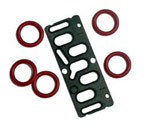
Seal, 0-ring (r) a product of precise dimensions molded in one piece to the configuration of a torus with circular cross section, suitable for use in a machined groove for static or dynamic service.
Secondary accelerator (r) accelerator used in smaller concentrations, compared to the primary accelerator, to achieve a faster rate of vulcanization.
Semiconductor (sc) a material whose electrical resistivity is intermediate between that of conductors and insulators, in which conduction takes place by means of holes and electrons.
Set (r) strain remaining after complete release of the force producing the deformation.
Shelf life (r) see storage life, shelf.
Shock load (r) the sudden application of an external force.
Shrinkage (r) 1) decrease in volume of a seal in service due to extraction of fillers. 2) decrease in volume of an elastomeric compound during molding.
Silicide (sc) a compound of silicon with a refractory metal. Common silicide semiconductor films (used as interconnects) include titanium, tungsten, tantalum and molybdenum.
Silicon dioxide (SiO2) (sc) a non-conducting layer that can be thermally grown or deposited on silicon wafers. Thermal silicon dioxide is commonly grown using either oxygen or water vapor at temperatures above 900°C.
Silicon nitride (Si3N4) (sc) a nonconductive layer chemically deposited on wafers at temperatures between 600° and 900°C.
Silicone rubber (r) poly dimethyl siloxane elastomer.
Solubility the ability or tendency of one substance to blend uniformly with another.
Sorption the term used to denote the combination of absorption and adsorption processes in the same substance.
Specific gravity the ratio of the weight of a given substance to the weight of an equal volume of water at a specified temperature.
Spew line (r) line on the surface of a molded product at the junction of the mold parts.
Spin-on-glass (SOG) (sc) a dielectric suspended in a liquid solvent at room temperature, allowing the material to be “spun” onto a wafer. Most SOG films are siloxane polymers dissolved in alcohol-ketone solvents. After being “spun” on the wafer, the wafers must be baked to drive off the solvent.
Sputtering (sc) a method of depositing a thin film of material on wafer surfaces. A target of the desired material is bombarded with radio frequency-excited ions which knock atoms from the target; the dislodged target material deposits on the wafer surface.
Squeeze (r) the compression of a seal, usually expressed as a percentage calculated by dividing the deformation by the original seal cross-sectional diameter.
Standard clean one (SC1) (sc) a mixture of ammonium hydroxide, hydrogen peroxide and UPDI. The first step in the RCA Cleaning process, which is designed to remove organic material.
Standard clean two (SC2) (sc) a mixture of hydrochloric acid, hydrogen peroxide and UPDI. The second step in the RCA Cleaning process, which is designed to remove metals and other inorganic material.
Static seal (r) a seal in which the sealing surfaces do not move relative to each other.
Steam oxide (sc) thermal silicon dioxide grown by bubbling a gas (usually oxygen or nitrogen) through water at 100°C.
Stepper (sc) a machine which steps a reticle directly onto the wafer. A reticle can be produced at lower defect level and with tighter dimensional control than an entire mask, resulting in wafer images having fewer defects. Alignment of reticle to wafer is accomplished by reflecting a laser beam through a special reticle pattern (alignment target) and off a corresponding pattern on the wafer.
Stiction (r) the increase in static friction resulting from prolonged seal compression.
Stiffness, bending (r) the force required to produce a bent configuration under specified conditions.
Stock (r) see compound.
Storage life, shelf (r) the period of time after production during which a material or product that is stored under specified conditions retains its intended performance capabilities.
Strain the unit change, due to force, in the size or shape of a body referred to its original size or shape.
Stress the intensity, at a point in a body, of the internal forces (or components of force) that act on a given plane through the point.
Stress relaxation (r) the decrease in stress after a given time at constant strain.
Stripping (sc) removal process; usually refers to photoresist.
Susceptor (sc) a component of many equipment systems on which the wafer is placed. Frequently made of high-purity graphite.
Swelling (r) the increase in volume of a specimen immersed in a liquid or exposed to a vapor.
(sc) This term is generally associated with the semiconductor industry.(r) This term is generally associated with the rubber industry.
Next T's
Our specialty is solving sealing problems for original equipment manufacturers. We carry o-rings, seals, custom molded rubber parts, wipers, diaphrams, valves and u-cups in all types of materials including Kalrez®, FKM fluorocarbon, Simriz®, nitrile (buna-n), silicone, rubber, neoprene, polyurethane, TFE and FEP encapsulated.
We are located in the Denver Technological
Center in a suburb of Denver, Colorado
©1997-2017, Problem Solving Products, Inc.
Website Map | Privacy Statement
| Terms of Use

